How Does a Silicon Focus Ring Improve Etch Uniformity?
-
 author
- 17th septembre 2026
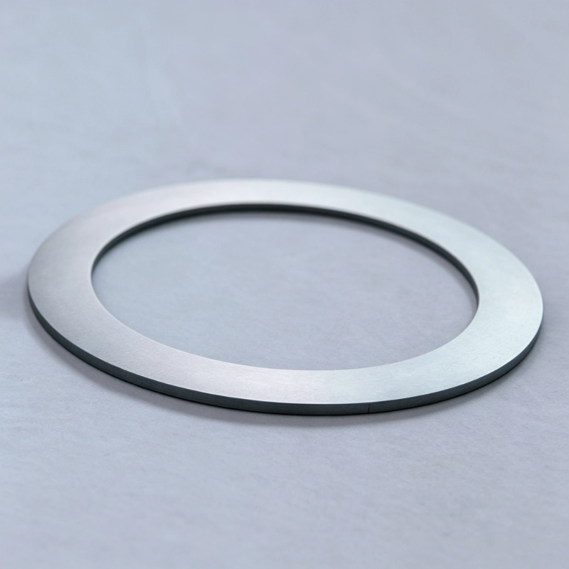
A silicon focus ring helps control the plasma boundary at the wafer edge, where the electrical and physical environment changes abruptly. By extending the process region beyond the wafer perimeter, the ring can reduce edge-to-center differences in ion arrival conditions and etch rate. Its effect depends on geometry, material properties, surface condition, and wear, so the ring must be treated as a process-matched consumable rather than a generic spare part.
Why Does the Wafer Edge Need a Focus Ring?
Inside a plasma etch chamber, most of the wafer sits above a comparatively regular electrode surface. At the outer edge, that continuity ends. The change in height, material, and electrical boundary can bend the plasma sheath, altering the angle and energy at which ions reach the surface. Even when the center process is stable, this boundary effect can produce a different etch profile near the perimeter.
A focus ring surrounds the wafer and creates a more controlled transition beyond that perimeter. The ring does not make the plasma uniform by itself. It gives the chamber and recipe a designed edge boundary, allowing the sheath and ion trajectories to remain closer to the conditions over the active wafer area. That is why ring geometry and chamber setup must be evaluated together.

How Does Silicon Focus Ring Geometry Affect Uniformity?
The most important geometric relationship is often the height of the ring surface relative to the wafer. If a silicon focus ring sits too high or too low, the sheath can curve near the edge and redirect ions. The resulting change may affect local etch rate, sidewall profile, or critical-dimension behavior. A new ring, a worn ring, and a ring installed with the wrong supporting stack can therefore produce different edge results even under the same nominal recipe.
The radial gap between the wafer and ring also matters. A large or uneven gap creates a discontinuity around the circumference, while poor concentricity makes that discontinuity vary by angle. Inner diameter, outer diameter, thickness, flatness, and step geometry should therefore come from the chamber drawing and the qualified part definition, not from wafer diameter alone.
Height and Wear Must Be Evaluated as One System
Plasma exposure gradually changes the ring surface and effective profile. As erosion lowers or reshapes the area nearest the wafer, the electric field and sheath at the edge can shift. Process teams should compare edge-uniformity data with ring age, measured wear, and chamber maintenance history. A fixed replacement interval is useful only when it reflects the actual recipe mix, power, chemistry, and acceptable process window.
Surface Finish Can Change More Than Appearance
Surface condition influences how reaction products accumulate and release. Scratches, machining damage, pits, or localized roughness on a silicon focus ring can change deposition behavior and become particle risks. The correct acceptance limit depends on the process position and equipment specification. Visual inspection alone may miss small dimensional or surface changes, so incoming measurements and post-run trend data should support the decision.
Why Choose Silicon for a Focus Ring?
Silicon is useful when process compatibility, electrical behavior, and contamination control favor a material closely related to the wafer. A silicon focus ring may use monocrystalline or polycrystalline material, but those options do not behave identically, and neither is automatically correct for every chamber. Material grade, resistivity, conductivity type, crystal orientation, and any coating must match the approved equipment configuration and process chemistry.
The current silicon ring product range from THE EQUATOR includes monocrystalline and polycrystalline options made to customer drawings. The supplier’s listed inspection fields include dimensions, material grade, resistivity, conductivity type, and visual condition. Buyers should treat those records as part of qualification evidence and confirm that every limit traces back to their own tool and recipe requirements.
What Should Buyers Specify Before Ordering?
Before ordering a silicon focus ring, a request for quotation should define the equipment model or controlled drawing revision, wafer size, ring function, material, resistivity range, conductivity type, and crystal orientation. It should also cover coating status, critical dimensions, surface finish, cleanliness method, packaging, and report requirements. When the original equipment specification is confidential, buyers can issue a controlled drawing or tolerance table that exposes only the information required for manufacturing and inspection.
The acceptance plan should distinguish dimensions that affect the plasma boundary from features that primarily support assembly. Inner diameter, wafer-to-ring gap, top-surface height, concentricity, flatness, and critical steps often deserve direct attention. Hole locations, chamfers, and contact surfaces can also matter when they affect gas flow, clamping, thermal contact, or installation repeatability.

THE EQUATOR’s quality testing services cover purity, resistivity, dimensional and positional tolerances, surface condition, and customized reports. Those capabilities are most valuable when the buyer first defines measurement methods, sampling rules, units, and pass/fail limits. A number without its method or drawing reference is difficult to compare across suppliers or lots.
How Should a Qualification Trial Connect the Ring to Process Data?
A qualification trial should isolate the part change as far as practical. Record the chamber state, clean history, recipe, wafer type, installed silicon focus ring measurements, and baseline edge performance before the trial. After installation, compare edge-to-center etch rate, profile or critical-dimension behavior, particle results, and any tool alarms across enough runs to separate initial conditioning from stable operation.
For customized parts, begin with a controlled sample lot and preserve serial or lot identity through incoming inspection and chamber use. The semiconductor equipment component solution is relevant when procurement needs a supplier to coordinate precision components for etching, PVD, or CVD equipment. Approval should still rest on the buyer’s measured process window, not on a catalog description alone.
FAQs
Q: Does a silicon focus ring guarantee uniform plasma etching?
A: No. The ring shapes the wafer-edge boundary, but uniformity also depends on chamber geometry, electrode condition, recipe, gas flow, power, wafer position, and ring wear. A correct part must be qualified with process data from the intended tool.
Q: Which dimensions matter most when specifying a silicon focus ring?
A: Inner diameter, wafer-to-ring gap, top-surface height, thickness, concentricity, flatness, and critical steps often influence edge conditions or installation. The controlling dimensions and tolerances must come from the equipment drawing and the validated process window.
Q: What should accompany a silicon focus ring sample lot?
A: The lot should include traceable material identification and the agreed inspection results, such as dimensions, resistivity, conductivity type, surface condition, and visual findings. Buyers should connect those records to chamber installation data and wafer-level trial results.


plaquettes de silicium
Anneau en silicone
tiges de silicone
Creuset en quartz
Pièces en graphite
Silicium polycristallin de qualité électronique (en vrac)

Faites appel à nous pour des solutions semi-conducteurs fiables.
Que vous ayez besoin de matériaux semi-conducteurs standard ou de spécifications techniques personnalisées, notre équipe d'ingénieurs experts est à votre disposition. Soumettez vos besoins dès maintenant et recevez un devis détaillé et professionnel sous 24 heures.
Demander un devis