How to Choose Wafer Polishing Consumables for Planarization
-
 作者
- 5th 11 月 2026
Put a pad quotation beside a wafer inspection map. The lower price looks less attractive if the trial leaves scratches near the edge. That’s where choosing wafer polishing consumables gets harder than comparing two price lists.
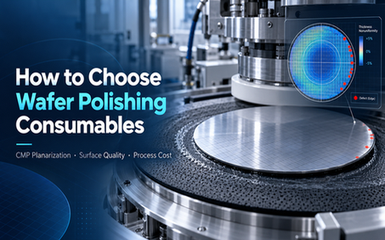
In semiconductor wafer manufacturing, chemical mechanical planarization (CMP) prepares the surface for what comes next. Leave too much unevenness and later patterning becomes harder. Remove too much and a layer meant to stay may suffer. Buying for CMP planarization means finding a combination that meets both limits on the actual production tool.
What Are Wafer Polishing Consumables?
Think of the contact beneath a rotating wafer. Slurry reaches the pad carrying abrasive particles; its chemistry helps make the exposed film removable. The pad supplies the working surface. Conditioning restores its texture as use changes it. Together they provide the chemical and mechanical action behind wafer planarization.
An order for polishing consumables might contain separate items. On the tool, though, a new slurry can change what the existing pad does. A purchase specification for each component won’t tell you whether their combination works.
Key Types of Wafer Polishing Consumables
CMP Slurry
Abrasive particles and chemistry both affect removal. Check the target film before comparing pH or particle characteristics. Oxide CMP and copper CMP need different approaches; barrier removal brings another selectivity requirement. An aggressive formulation is useful only if it leaves the required surface behind.
CMP Polishing Pads
A softer pad can follow local topography more readily. That may suit a finishing step but compromise the planarization you need elsewhere. For a CMP polishing pad, compare pore structure and slurry transport too. Check results after break-in and again near the planned replacement point.
CMP Pad Conditioners
A CMP pad conditioner maintains the pad’s working texture. Too little conditioning can let it glaze. Excessive conditioning can consume the pad faster. Match the conditioner to the pad and check the conditioning settings during trials.
Other Related Consumables
Retaining rings affect edge behavior. Filters help control particles in slurry delivery. Post-CMP cleaning consumables remove residues after polishing. Include these in defect troubleshooting when changing the main CMP consumables fails to resolve the problem.
Five Factors to Consider When Choosing Wafer Polishing Consumables
1. Wafer Material and Target Film
“For silicon wafers” leaves a lot unsaid. Are you removing silicon itself or a deposited oxide? Is tungsten exposed? Copper needs different chemistry again. Give the supplier the film stack and the layer that must remain. “For semiconductor wafer polishing” is too broad a purchasing specification.
2. Material Removal Rate and Selectivity
For a 600 nm target, the arithmetic looks tempting. A constant rate of 200 nm/min gives three minutes under polish; 300 nm/min gives two. These are assumed trial figures. The loading cycle hasn’t shortened, though. Neither has cleaning. The throughput forecast needs those times as well.
Selectivity can undo the apparent gain. How much of the underlying film disappears while you reach the target? Put that loss beside the faster rate before calling it an improvement.
3. Surface Quality and Defect Control
Look beyond a smooth average roughness reading. A scratch may still fail inspection. Dishing means metal sits recessed; erosion concerns the loss across a patterned region. Neither disappears into an average. Write down the limits for surface-defect checks before testing. Within-wafer nonuniformity needs a number and a wafer map. Don’t let a respectable average conceal an edge problem.
4. Equipment Compatibility and Process Stability
Will the proposed pad fit the platen? Does the setup suit your wafer diameter? Resolve those basic questions before discussing removal targets. Check slurry delivery and conditioning settings under the intended operating conditions. Change a pad and slurry together and a bad trial gives you two suspects. Retain the qualified setup as a reference.
At the tool, compare a wafer taken just after pad break-in with one processed near the planned pad change. Keep inspection conditions identical. Extra cleaning on the later wafer belongs in the qualification record. So does a change in its edge profile. Otherwise the quotation leaves out part of the job.
5. Total Cost of Ownership
Take an assumed $300 pad that produces 1000 accepted wafers: $0.30 of pad cost per wafer. A $240 pad delivering 600 costs $0.40 per accepted wafer. The cheaper purchase has become the dearer option. There’s still the time spent replacing it. Slurry use can move the bill again, along with cleaning or waste handling. Work those costs into the trial review.
How to Evaluate a Wafer Polishing Consumables Supplier
Verify Quality and Batch Consistency
A certificate of analysis can look reassuring without answering the question that matters to your process. Compare its measurements with the agreed specification. Check inspection reports against the same method. Retain the lot identity on the trial record; you’ll want it if the next delivery behaves differently.
Confirm Technical and Supply Capabilities
Use a small trial order to establish process fit. Confirm product-specific compatibility before qualification. Carry the accepted specification and lot identity into the next purchase. Put delivery dates into the replenishment plan, including the time needed to inspect incoming material. Ask about formulation changes too. You need enough notice to decide whether another trial is necessary.
Common Mistakes to Avoid When Selecting CMP Consumables
A lower quotation can hide a shorter working life. Swapping slurry while treating the pad as irrelevant is another expensive shortcut. Supplier comparisons also fall apart when each trial uses different settings.
The container deserves a look too. Material waiting on a shelf is still aging. Check its expiry date and storage history before blaming a changed recipe. One passing wafer leaves the next lot’s behavior untested. Allow for repeat runs before scaling up.
A Practical Checklist for Buyers
Record wafer material and diameter with the target film.
Define removal rate and selectivity.
Set surface-quality and defect limits.
Verify consumable fit on the intended equipment.
Match quality documents to the lot being purchased.
Book sample trials and allow for supply lead times.
Compare total cost per accepted wafer.
常見問題解答
What Are the Main Consumables Used in CMP?
You’ll be buying slurry alongside a pad and its conditioner. Budget for the retaining ring too. Filtration and post-CMP cleaning belong in the purchasing scope wherever the process requires them.
How Do I Choose the Right CMP Slurry?
Begin with the exposed film and required selectivity. Test removal rate against defect limits using the intended pad. A slurry specification alone cannot establish process fit.
How Can I Reduce the Cost of Wafer Polishing?
Track cost per accepted wafer. Longer pad life helps only while quality stays within limits. Check what you spend during a whole pad run before negotiating another discount.
Conclusion: Choose Consumables Based on Process Requirements
The trial has to answer the buying question: does this combination do the job on your tool? Keep its conditions with the purchasing specification. For sourcing support, send THE EQUATOR your application requirements with the target film and tool details. Include your acceptance limits and supply schedule so we can work from a useful starting point.


矽晶片
矽膠環
矽膠棒
石英坩堝
電子級多晶矽(塊狀)

與我們合作,取得可靠的半導體解決方案。
無論您需要標準半導體材料還是客製化技術規格,我們的專家工程團隊都隨時準備為您提供協助。立即提交您的需求,即可在 24 小時內收到詳細專業的報價。
索取報價