What Does Wafer TTV Tell You Before a Process Trial?
-
 作者
- 29th 10 月 2026
At goods receiving, a label reads “TTV < 3 um.” Someone sets the report beside last month’s batch. The old report says 3 um too. Neither has a point map. Same stamp. Same limit. The numbers look comparable until someone asks how each lab took them.
Wafer total thickness variation (TTV) is the difference between the thickest and thinnest measured points under a stated method. It tells you thickness spread. It does not describe bow. Nor does it tell you about warp or surface roughness. The number alone cannot confirm process fit.
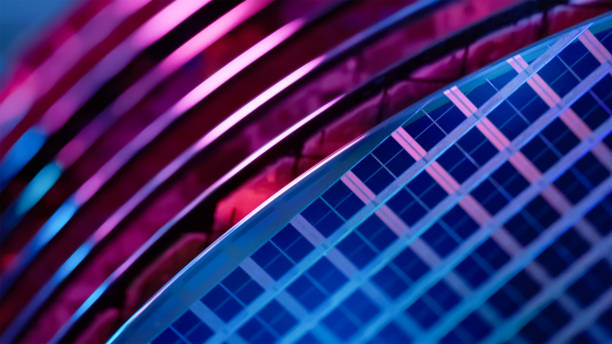
What Does Wafer TTV Measure Across the Disc?
TTV is a range. Take the highest thickness reading in the defined measurement area and subtract the lowest. The answer is the total thickness variation for those measured points.
Take two points on a sample map. At one point the gauge reads 725.4 um. At another it reads 723.0 um. Subtract the second from the first and the map’s TTV is 2.4 um. I chose those figures to make the math visible. They are not a production reading.
The map matters. Two wafers can have the same TTV while the high and low points sit in different places. One report might sample the center and edge. Another might use a denser pattern. The headline value hides that difference.
When someone hands you a “3 um max” spec, ask what area was measured and how the points were selected. Without that context, the figure is hard to compare with last month’s report.
How Does Wafer TTV Differ from Bow and Warp?
TTV is the odd one out because it describes a thickness range. Bow and warp concern the wafer’s shape. Roughness? That is the finish at the surface.
Bow measures how far the center of an unsupported wafer sits from a reference plane. Warp looks across more of the wafer’s surface to describe its out-of-plane shape. Close cousins, but still separate readings.
For our 矽晶片系列, TTV is controlled below 3 um. Bow stays under 20 um. Warp stays below 25 um. I would not fold those into a single “flatness” score. They refer to different measurements. None becomes a blanket acceptance limit for every process.
Our surface roughness figure can reach 0.1 nm. Convert 3 um to 3,000 nm and the scale difference feels less abstract. Still, these are separate properties. A polished face can be smooth while thickness changes from center to edge. For a scratch or particle, ask for surface roughness and defect checks. A TTV number will not show it.
When Does Silicon Wafer TTV Matter in a Process Tool?
TTV is easiest to read by itself. It gets more interesting when the wafer meets a chuck or the step that holds it against something flat. The support condition changes the question. Bow and warp can explain behavior that a thickness range cannot.
Picture a wafer pulled onto a vacuum chuck. TTV is only one piece of that contact. A clean number can sit beside a bowed wafer; they describe different things. The tool’s design and correction range matter too.
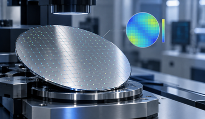
Focus and height control create another reason to keep the terms separate. A TTV number can help screen incoming wafer geometry. It is not a focus map and cannot tell the team how much correction remains during a particular step.
Bonding and precision grinding bring their own concerns. The team may care about thickness through a stack or across a working pass. Three micrometers sounds neat on a spec sheet. Is that the right limit? Not until you know which step it needs to protect.
Start from the miss you want to catch. I’d be wary of a tighter limit when receiving and the supplier measure different patches.
How Should You Read a Wafer TTV Report?
Put the report beside the purchase specification. Then check whether the two describe the same wafer and the same measurement.
Does the wafer diameter and nominal thickness match the incoming spec? The report header should settle that quickly.
Where are the high and low readings? If there is no point map, ask for it.
Was the wafer free during measurement or held against a support? That difference belongs in the record.
Bow and warp need their own entries. They are not TTV.
A lot number and an inspection date keep the report attached to the right batch.
Sometimes the headline value is on one sheet and the map is in another file. Keep them together. Two reports can both read 2.9 um yet refer to different points on the wafer.
Our dimensional and flatness testing can help settle the geometry side. Tell us what was held in the fixture and which point pattern matters. A report read three months later should still tell you which sample it came from.
What Should You Confirm Before Setting a Wafer TTV Limit?
The acceptance limit needs the wafer size and nominal thickness beside it. The report should say where the measurements were taken. What was supporting the wafer? That belongs in the record too. Keep bow and warp on their own lines when the process needs both.
If you are comparing two reports that both say “under 3 um” but still cannot tell whether the wafers are comparable, send us the measurement setup. Include the process step and what the team needs the limit to prevent. We can start with those details.
常問問題
These are the questions worth asking before anyone changes the limit.
Is TTV Equivalent to Wafer Flatness?
No. TTV is a thickness range. Flatness concerns the wafer’s shape against a reference. A small TTV can sit alongside a curved wafer, so check both when the tool depends on seating.
Can Low TTV Still Come with Wafer Bow?
Yes, it can. TTV tracks thickness. Bow describes the wafer’s curve when it is free. If seating matters to your process, keep the bow result beside the TTV reading.
Does a 3-Micrometer TTV Limit Fit Every Wafer Size?
No. A 2-inch wafer and a 12-inch wafer do not pose the same geometry question. Thickness and support condition enter the decision too. Set the number against the process step; a limit copied from another setup can miss the problem you meant to catch.
Is Surface Roughness Part of Wafer TTV?
No. Roughness is the finish at the surface. TTV is thickness from high to low. Put them on separate lines; a texture reading cannot replace the map.

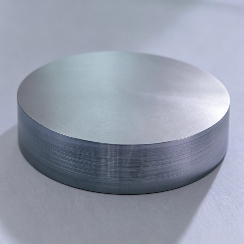
矽晶片
矽膠環
矽膠棒
石英坩堝
電子級多晶矽(塊狀)

與我們合作,取得可靠的半導體解決方案。
無論您需要標準半導體材料還是客製化技術規格,我們的專家工程團隊都隨時準備為您提供協助。立即提交您的需求,即可在 24 小時內收到詳細專業的報價。
索取報價