High-purity silicon processed parts
Including precision-machined components such as silicon electrodes, silicon rings, silicon boats, and silicon baffles, it adopts advanced MCZ silicon materials and micro-hole processing technology, with precision controlled within 0.3mm and polishing precision below 0.1μm, suitable for key processes such as etching and diffusion.
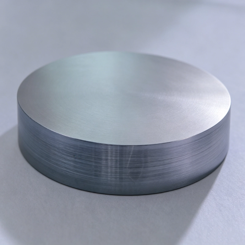
silicon wafers
Silicon wafers are thin, round wafers made from high-purity single-crystal silicon rods through precision processing including cutting, grinding, etching, and polishing. They are the fundamental substrate material for semiconductor chip manufacturing. As the carrier of integrated circuits, silicon wafers have billions of transistors and interconnects formed on their surface through processes such as photolithography, etching, deposition, and ion implantation. Finally, they are diced and packaged into chips. The purity, flatness, surface cleanliness, and crystal quality of silicon wafers directly determine the yield rate and device performance in chip manufacturing.
Our company's silicon wafers are made from high-purity single-crystal silicon rods produced by advanced MCZ farad technology, through processes such as multi-wire cutting, double-sided grinding, chemical etching, and precision polishing. The product purity can reach over 99.9999999%, the flatness (TTV) is controlled below three micrometers, and the surface roughness can be as low as 0.1 nanometers. Product diameters range from two inches to twelve inches, offering various types including polished wafers, annealed wafers, and epitaxial wafers. Customized silicon wafers with different conductivity types, resistivity ranges, and crystal orientations can also be provided according to customer needs.
Learn More
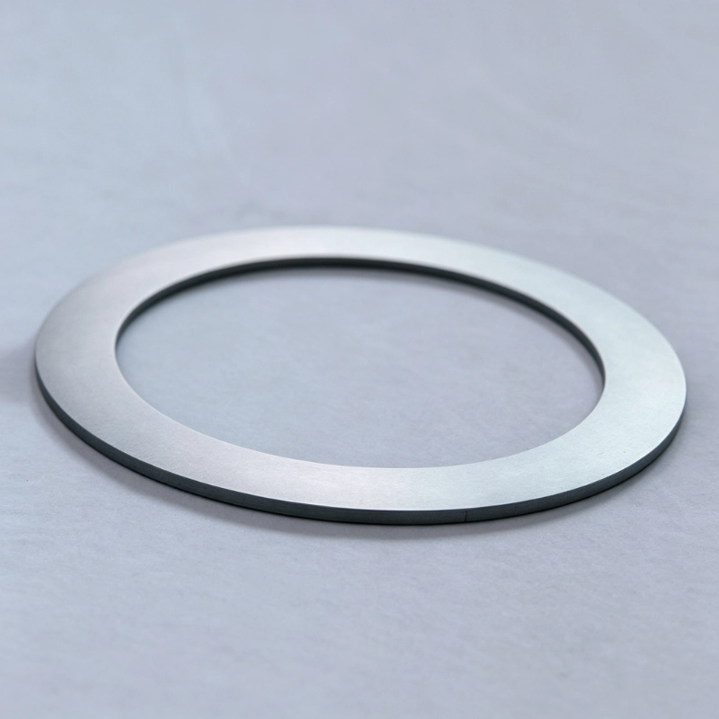
Silicon ring
Silicon rings are ring-shaped silicon components made from high-purity single-crystal or polycrystalline silicon through precision machining. They are key consumable components in semiconductor etching and plasma processing equipment. Silicon rings are typically installed in the reaction chambers of semiconductor process equipment such as plasma etching machines, physical vapor deposition (PVD) machines, and chemical vapor deposition (CVD) machines, serving to focus plasma, protect the inner walls of the chamber, uniformize the electric field distribution, and control process uniformity. Silicon rings utilize the high purity, plasma corrosion resistance, and excellent thermal and electrical conductivity of single-crystal silicon to maintain stable physicochemical properties in harsh plasma environments.
Our company's silicon ring products use high-purity single-crystal or polycrystalline silicon produced by advanced MCZ farad technology. They are manufactured through multiple precision machining processes including cutting, grinding, drilling, and polishing, achieving a purity of over 99.99999999%, dimensional accuracy within ±0.1 mm, and surface roughness below 0.1 micrometer. Product specifications cover various sizes of focusing rings, protective rings, and edge rings for 2-inch to 12-inch etching equipment, and custom designs are also available.
Learn More
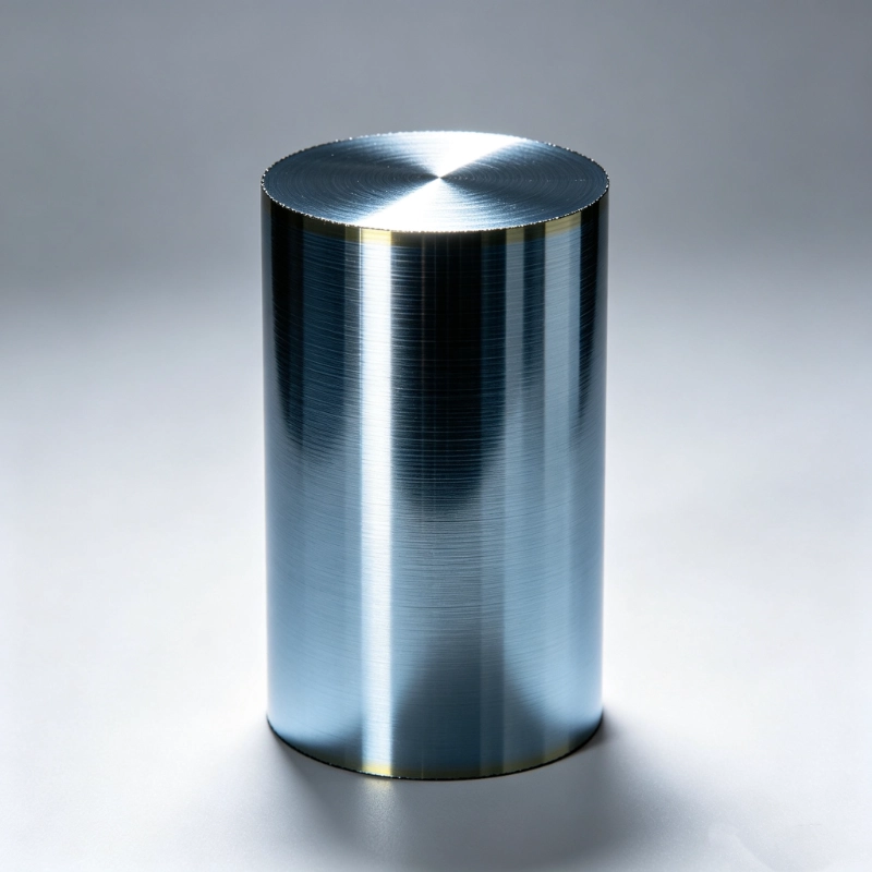
Silicon rods
Silicon rods are high-purity cylindrical silicon crystals grown using the Czochralski (CZ) or zone melting methods, and are a core material in semiconductor wafer manufacturing. Silicon rods are made from electronic-grade polycrystalline silicon, which is melted at high temperatures and then guided by seed crystals under controlled growth conditions to form single-crystal silicon rods with a complete crystal structure or polycrystalline silicon rods composed of multiple grains. Single-crystal silicon rods have a uniform crystal orientation and a defect-free lattice structure, making them suitable for substrate manufacturing of high-end semiconductor chips such as integrated circuits and power devices. Polycrystalline silicon rods, due to their cost advantage, are mainly used in photovoltaic cells and some low-end semiconductor devices. Our company's silicon rods are grown using advanced MCZ (Magnetic Czochralski) technology, with resistivity uniformity controlled within 5% and purity exceeding 99.9999999%. Product diameters range from two inches to twelve inches, and we can provide customized silicon rods with different conductivity types (N-type/P-type), resistivity ranges, and crystal orientations according to customer needs.
Learn More
Frequently Asked Questions
Do you support small-batch purchases?
Yes, we accept sample orders, small-batch trial orders, and large-batch orders, flexibly adapting to different needs such as R&D prototyping and mass production preparation.
Can you provide product samples?
A home solar storage system costs between $5,000–$15,000 on average, depending on capacity and brand. Rebates and incentives can lower this cost.
the product quality guaranteed?
All products are sourced from reputable manufacturers. Strict verification of specifications and purity is performed upon receipt. Factory inspection reports are available, ensuring stable and compliant quality.
Can you provide material certificates and purity reports?
Yes, we can provide complete material certificates, purity test reports, and relevant shipping documents after ordering.
Can you help source scarce semiconductor materials?
Yes, leveraging industry resources, we can assist in sourcing discontinued, scarce, and special-specification semiconductor-related materials and accessories.
Do you support customized sizes and specifications?
Yes, we support custom processing based on customer drawings, dimensions, and precision requirements, connecting with the original manufacturer.

Partner with us for reliable semiconductor solutions.
Whether you need standard semiconductor materials or custom technical specifications, our expert engineering team is ready to help. Submit your requirements now and receive a detailed, professional quote within 24 hours.
Request A Quote