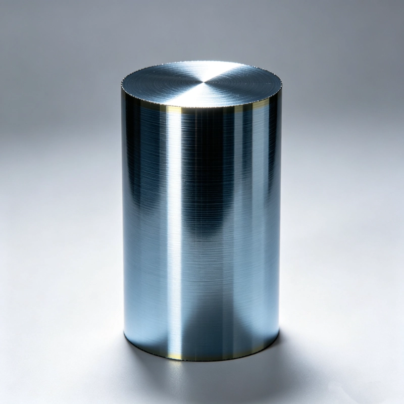
Silicon rods
Product Details
a) Product Features and Advantages
Ultra-high purity standard
All our silicon ingots start with electronic-grade polysilicon raw materials. We tightly regulate crystal pulling procedures to secure purity above 9N. Donor impurities stay below 0.15 ppba, acceptors under 0.10 ppba, while carbon and oxygen are limited to 0.05 ppma at maximum. This ultra-clean base material guarantees outstanding electrical performance and low defect rates on sliced silicon wafers for downstream chip production.
Even resistivity across the whole ingot
We adopt MCZ magnetic crystal pulling tech. Magnetic fields restrain liquid silicon convection, distributing dopants far more evenly. Our ingots keep radial resistivity deviation within 5%, with mild axial fluctuation. Stable resistivity offers uniform processing conditions for buyers and helps lift finished chip yield rates.
Low internal micro-defects
We fine-tune thermal field layout, pulling speed and crystal rotation parameters during production. This cuts dislocation and tiny crystal defects inside ingots significantly. Complete crystal structures prevent surface flaws during later polishing and epitaxy steps, making wafers qualified for advanced processes like 7nm and 14nm node substrates.
Multiple crystal growth options on hand
We supply ingots made via different pulling methods to match diverse production demands.
CZ monocrystalline ingots: mainstream choice for ICs and power semiconductor manufacturing
- Float zone ingots: ultra-low oxygen and higher purity, fit high-voltage power parts and radio frequency chips
- Polycrystalline ingots: cost-effective, mainly for solar cell production and special custom uses
Fully customizable specifications
We tailor silicon ingots fully based on your factory process demands. Adjustable options include N/P conductivity type, wide resistivity range (0.001 up to 10,000 ohm·cm), crystal plane orientations (100 / 110 / 111 etc.), diameters from 2 to 12 inches and custom lengths. Our technical team can give targeted material selection suggestions after learning your application scenarios.
Stable quality between batches
We run full-process quality checks from polysilicon incoming inspection to finished rod testing. Every batch goes through dimension measurement, resistivity scanning and impurity analysis; all test records are fully traceable. We maintain long-term stable supply channels with top domestic polysilicon manufacturers, with large-scale production capacity. Consistent batch quality lowers your incoming inspection workload and avoids unstable production from material differences.
Complete test reports and third-party inspection support
Every silicon rod comes with full test documents covering dimensions, resistivity distribution, doping type, impurity levels, crystal orientation and dislocation density. We welcome clients to arrange third-party labs for re-inspection. Our engineers also provide technical guidance to help you verify materials and match your production lines smoothly.
b) Product Parameters
Item name: Silicon rod (monocrystalline / polycrystalline available)
- Production process: Mono rods adopt CZ or float zone melting; poly rods use directional solidification casting
- Shape: Cylindrical
- Standard diameters: 2 / 3 / 4 / 6 / 8 / 12 inches; custom sizes acceptable
- Diameter tolerance: ±0.5 mm; 8-inch and larger rods controlled within ±0.3 mm
- Length: Standard 1–2 meters, adjustable as requested
- Conductivity type: N-type (phosphorus / arsenic / antimony doping) or P-type (boron doping)
- Resistivity range: Low resistance: 0.001–0.1 ohm·cm Medium resistance: 0.1–100 ohm·cm High resistance: 100–10,000 ohm·cm, fully customizable
- Resistivity uniformity for MCZ mono rods: Radial ≤5%, axial fluctuation ≤15%
- Crystal orientation: Standard 100 / 110 / 111, custom special orientations supported
- Purity standard: Mono silicon ≥9N; poly silicon ≥6N
- Impurity limits: Donor ≤0.15 ppba, Acceptor ≤0.10 ppba CZ mono: C ≤0.05 ppma, O ≤0.05 ppma Float zone mono: O ≤0.01 ppma
- Dislocation density: Below 500 pcs/cm²
- Minority carrier lifetime: N-type >1000 μs; P-type >500 μs
- Delivery document: Full test report attached for each rod, covering all above core indexes
Application Fields
- Integrated circuit wafer production Monocrystalline ingots go through slicing, grinding and polishing to become base wafers for logic, memory and analog chips. We supply full-size rods: 6-inch for mature manufacturing lines, up to 12-inch for advanced tiny-node processes.
- Power semiconductor components Wafers cut from mono rods make power diodes, MOSFET and IGBT devices. Float zone silicon features ultra-low oxygen and high resistivity, perfect for high-voltage thyristors, high-power IGBT modules and other heavy-duty electronic parts.
- MEMS & sensor manufacturing Uniform crystal structure and controllable crystal planes make mono rods ideal MEMS substrates. They are widely used in accelerometers, gyroscopes, pressure sensors and micro mirror arrays; crystal orientation and resistivity directly decide device stability and finished yield.
- Solar cell production Polycrystalline rods and solar-grade mono rods are core raw materials for photovoltaic panels. After slicing, diffusion, coating and printing, silicon wafers turn into solar cells then assembled into modules. Mono silicon share keeps rising with high-efficiency cell technologies popularized.
- Spare parts for semiconductor equipment Custom-sized silicon rods can be processed into silicon rings, boats, electrodes and baffles used in etching, diffusion and epitaxy machines. The material’s high purity, plasma resistance and stable thermal performance extend service life of core equipment parts.
- Laboratory material research & new product development High-purity customized doped silicon rods with specific crystal planes support material research, new chip prototype testing and epitaxial substrate development. We accept small-batch multi-spec orders to assist your R&D projects.
Frequently Asked Questions
Q: What’s the difference between CZ silicon rods and float zone rods? How to pick the right one?
A: CZ rods melt polysilicon inside quartz crucibles and pull single crystals upward with seed crystals. They carry moderate oxygen content, strong mechanical strength, support large diameters and cost less. This is the mainstream material for most IC and regular power devices. Float zone rods heat local areas of polysilicon to form molten zones, which move upward to form single crystals without crucibles. Oxygen content stays extremely low, purity and resistivity uniformity are superior, yet maximum diameter is limited under 6 inches with higher costs. It fits high-voltage, high-power and oxygen-sensitive radio frequency chips. Suggestion: Choose CZ rods for common integrated circuits and regular power devices; float zone rods are recommended for devices above 1200V, high-power thyristors and RF products.
Q: What separates N-type and P-type silicon rods?
A: N-type silicon mixes pentavalent dopants like phosphorus and arsenic, electrons act as main charge carriers with fast electron mobility. P-type uses boron doping, holes become majority carriers. Chip factories select types based on device layout. P-type wafers dominate traditional CMOS lines due to mature process and lower cost. Confirm your chip design and production habits before placing orders.
Q: How does silicon rod resistivity affect finished device performance?
A: Resistivity decides silicon conductivity and directly impacts final electrical performance. Low resistance (0.001–0.1 ohm·cm): Heavy-doped substrates for power devices and epitaxy base wafers Medium resistance (0.1–100 ohm·cm): Standard choice for mainstream logic, memory and analog chips High resistance (100–10,000 ohm·cm): For high-voltage equipment, RF chips and precision sensors; float zone rods can reach extra high resistivity over 10,000 ohm·cm Match resistivity parameters according to your device design and process window.
Q: Why does crystal orientation matter for silicon rods?
A: Crystal orientation describes internal lattice arrangement marked by Miller indices such as 100, 110 and 111. Different orientations carry different atomic density and chemical activity, altering oxidation rate, epitaxy quality and carrier mobility in downstream steps. 100 plane is widely used in CMOS chips for low interface defect density; 110 suits certain power semiconductors and MEMS sensors; 111 mainly serves epitaxial substrates and special devices. We produce rods with designated crystal planes as required.
Q: What tolerance do you control for rod diameter?
A: Standard rods maintain diameter error within ±0.5 mm. For 8-inch and larger sizes, we tighten tolerance to ±0.3 mm. Precise dimension control avoids wafer edge defects and raw material waste during slicing.
Q: What’s your MOQ and delivery cycle?
A: Minimum order differs by diameter and resistivity specs. Standard items usually require 1–2 rods; custom parameters may need larger batches. Standard stock goods take 14–28 working days after deposit confirmation; fully customized rods need 4–6 weeks. Actual lead time changes with order quantity, specs and stock status, consult our sales team to lock the schedule in advance.
Q: Can I get samples for lab testing?
A: Sample supply is available for customer verification. We normally provide small 2/3-inch rod segments or test wafers. Sample quantity is limited, contact sales staff to go through application formalities. Our technical team also offers process matching guidance during sample testing.
Q: How do you guarantee consistent quality across all batches?
A: We adopt full-link quality control covering raw material screening, crystal pulling, cutting processing and finished testing. Every batch undergoes repeated tests on resistivity, doping type, impurity content, crystal plane and dislocation density, with all records traceable. We cooperate steadily with major domestic polysilicon suppliers to stabilize raw material quality and reduce batch fluctuation interference.

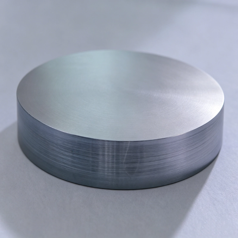
Silicon Wafers
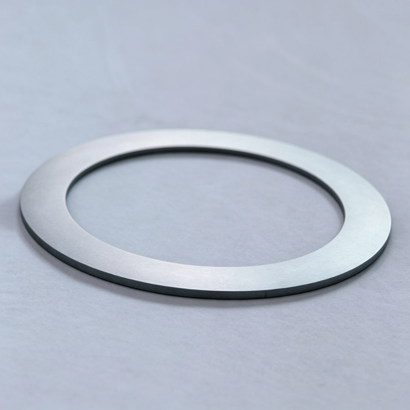
Silicon ring
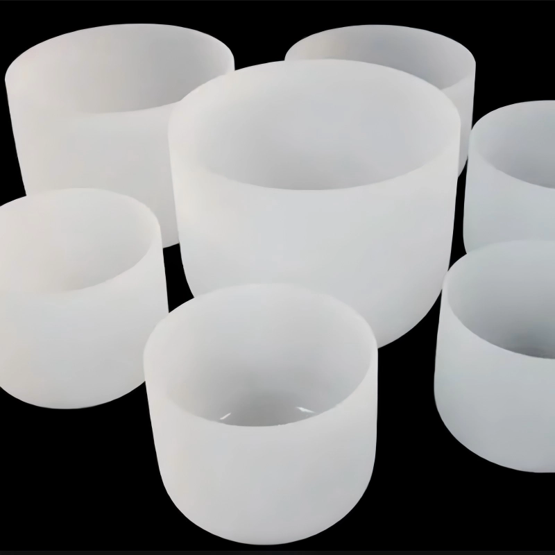
Quartz crucible
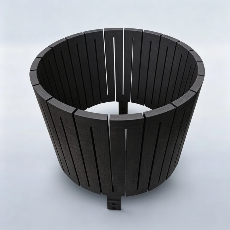
Graphite parts
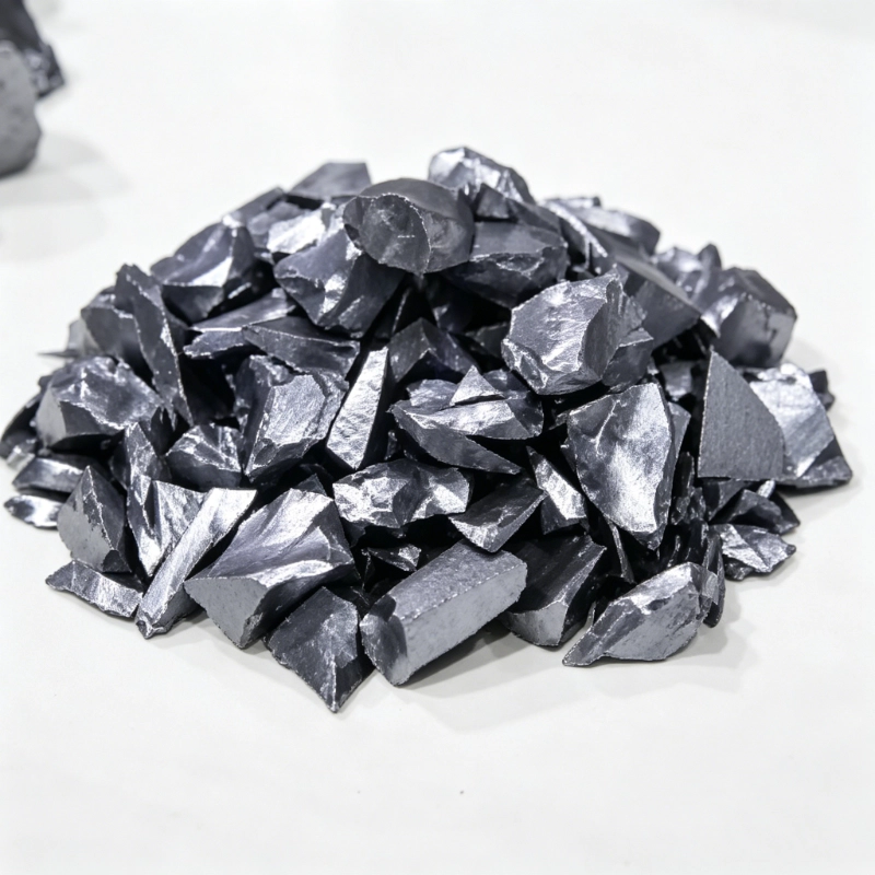
Electronic-grade polycrystalline silicon (bulk)
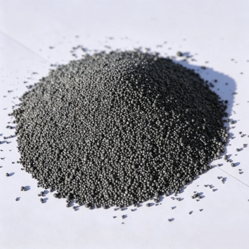
Electronic-grade polycrystalline silicon (particles)
News & Announcements
Recent Articles
 15th October 2026
Can a Small Batch Qualify Semiconductor Raw Materials?
 8th October 2026
Why Does Electronic Grade Polysilicon Price Vary?
 2nd October 2026
What Purity and Resistivity Data Should a High Purity Silicon Ingot Provide?
 10th September 2026
How Does a Quartz Crucible Affect Purity During Semiconductor Crystal Pulling?
 23rd September 2026
Why Does Silicon Wafer Price Vary for 8- and 12-Inch Sizes?
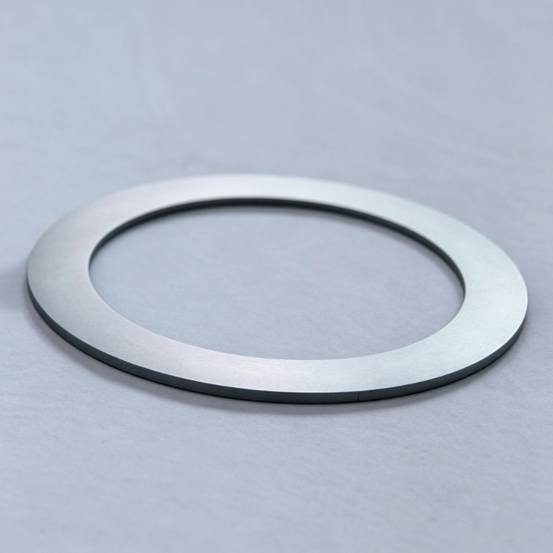 17th September 2026
How Does a Silicon Focus Ring Improve Etch Uniformity?
Our Service
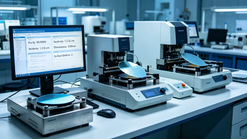
Quality testing services
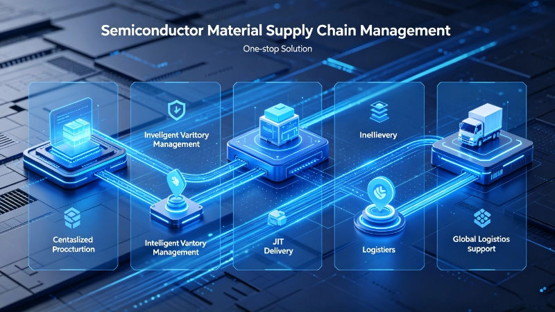
Supply chain management services

Partner with us for reliable semiconductor solutions.
Whether you need standard semiconductor materials or custom technical specifications, our expert engineering team is ready to help. Submit your requirements now and receive a detailed, professional quote within 24 hours.
Request A Quote