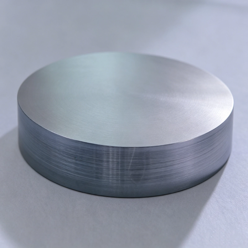
Silicon Wafers
Our company's silicon wafers are made from high-purity single-crystal silicon rods produced by advanced MCZ farad technology, through processes such as multi-wire cutting, double-sided grinding, chemical etching, and precision polishing. The product purity can reach over 99.9999999%, the flatness (TTV) is controlled below three micrometers, and the surface roughness can be as low as 0.1 nanometers. Product diameters range from two inches to twelve inches, offering various types including polished wafers, annealed wafers, and epitaxial wafers. Customized silicon wafers with different conductivity types, resistivity ranges, and crystal orientations can also be provided according to customer needs.
Product Details
a) Product Features and Advantages
Ultra clean high purity with few crystal defects
We make our wafers starting with electronic-grade polysilicon. The MCZ single crystal rods we pull hit purity above 9N, with carbon and oxygen strictly kept at ultra-low levels. We tweak crystal pulling processes to cut micro-defects and dislocation density inside wafers, creating premium base material for advanced chip fabrication. Traces of iron, copper, aluminum, calcium, sodium and other metal impurities are controlled down to ppb levels, so wafer surface cleanliness meets all semiconductor production standards.
Precise flatness and stable geometric dimensions
We adopt advanced multi-wire cutting and double-side grinding equipment to deliver top-tier flatness. TTV stays under 3 μm, bow below 20 μm, warp under 25 μm. Tight control over these geometric values keeps the focal plane steady during lithography and etching, which effectively raises finished chip yield.
Multiple surface finish options for different uses
We supply wafers with various surface treatments to match different production lines.
- Polished wafers: Treated with full CMP polishing, surface roughness Ra under 0.1 nm with zero damaged layer; fits most IC manufacturing.
- Annealed wafers: Go through high-temperature heat treatment to reduce oxygen precipitation and thermal donor issues, improving substrate electrical uniformity.
- Epitaxial wafers: A thin single silicon film grows on polished wafer surfaces. They carry fewer defects and offer highly precise resistivity control, ideal for power and RF chips with strict substrate standards.
Fully customizable specs
We adjust wafer parameters to match your exact production needs. Customizable items include N/P conductivity type, resistivity range (0.001 up to over 10,000 ohm·cm), crystal orientations (100 / 110 / 111), diameters from 2” to 12”, thickness, surface style and edge shaping. Our technical team can recommend suitable material solutions after learning your product application.
Strict whole-process cleanliness management
Wafers are produced in clean rooms ranging from Class 1000 to Class 100. Every working step follows strict particle control rules. Final wet cleaning removes surface particles, metal ions and organic residues thoroughly. Every piece gets surface particle and metal impurity testing to meet industry specs. Goods are vacuum sealed before shipment to avoid contamination during transit and storage.
Consistent quality across every batch
We run full quality control covering raw material screening all the way to finished wafer inspection. Each batch gets full geometric measurement, surface defect scanning and electrical performance testing, with all test data fully traceable. Standardized production lines and steady polysilicon supply keep batch quality uniform. This lowers your incoming inspection workload and prevents production swings caused by inconsistent material quality.
Complete test documents & third-party inspection allowed
Every batch ships with full test reports covering all core indexes: geometry (diameter, thickness, TTV, bow, warp), surface state (particle count, scratches, pits), electrical performance (doping type, resistivity, carrier lifetime) and impurity levels (oxygen, carbon, heavy metals). You may arrange third-party labs for rechecks as needed, and our engineers offer technical guidance for material validation and process matching.
b) Product Parameters
Product: Silicon wafer (monocrystalline / polycrystalline options)
- Raw material: Mono wafers cut from CZ single crystal rods; poly wafers cut from polycrystalline ingots
- Shape: Round thin wafer with shaped edges; edge options: primary flat, secondary flat, V-notch
- Standard diameters: 2”(50mm) / 3”(76mm) / 4”(100mm) / 6”(150mm) / 8”(200mm) / 12”(300mm); custom sizes available
- Diameter tolerance: ±0.2 mm
- Standard thickness & tolerance 6-inch: 500–700 μm 8-inch: 600–800 μm 12-inch: 700–850 μm Thickness tolerance: ±15 μm
- Geometric indexes TTV ≤3 μm, bow ≤20 μm, warp ≤25 μm 12-inch wafer SFQR flatness ≤0.13 μm, edge roll-off fully controlled
- Surface types: Single-side polished, double-side polished, annealed, epitaxial Polished wafer Ra < 0.1 nm Epitaxial layer thickness customizable: 2–10 μm, layer resistivity adjustable on request
- Surface particle standard: For 8-inch & larger wafers, particles above 0.13 μm ≤50 pcs per wafer
- Doping type: N-type (P / As / Sb doped); P-type (B doped)
- Resistivity range Low: 0.001–0.1 ohm·cm Medium: 0.1–100 ohm·cm High: 100–10,000+ ohm·cm Resistivity tolerance: ±10%
- Minority carrier lifetime: N-type >1000 μs; P-type >500 μs
- Crystal orientation: Standard 100 / 110 / 111, custom orientations supported
- Impurity limits Oxygen: 1.0×10¹⁷ ~ 1.4×10¹⁸ cm⁻³ Carbon: <5.0×10¹⁵ cm⁻³
- Delivery: Each batch comes with full test reports covering geometry, surface quality, electrical properties and impurity data
Application Areas
- Logic chip production Wafers act as core substrates for CPUs, GPUs, mobile processors and MCUs. Advanced nodes like 3nm and 5nm demand ultra-flat, clean, low-defect wafers. Our polished and annealed wafers fit both mature and cutting-edge logic chip lines.
- Memory chip manufacturing DRAM and 3D NAND require billions of memory units on wafer surfaces. Geometric stability and surface quality are critical, especially for stacked 3D NAND where wafer flatness directly affects multi-layer film deposition uniformity. Our wafers satisfy strict mass memory production standards.
- Power semiconductor components Diodes, MOSFETs, IGBT and silicon carbide modules mostly adopt heavily doped substrates with thin light-doped epitaxial layers. Epitaxial wafers are the mainstream pick here thanks to precise resistivity and low defects. We supply epitaxial wafers suited for 600V up to 1200V+ power devices.
- Analog & mixed-signal chips These chips need even wafer resistivity and long minority carrier lifetime to guarantee matching accuracy and low noise. Our high-quality CZ and float zone wafers meet such production demands.
- MEMS & sensor manufacturing MEMS devices like pressure sensors and accelerometers rely on specific crystal planes (111 widely used). We customize wafer crystal orientation to match unique MEMS process requirements.
- Photodetectors & solar cells Wafers also serve optical detection and photovoltaic production. Solar-grade wafers relax purity and geometry standards for better cost efficiency. We offer multiple purity grades to fit different budget and performance targets.
Frequently Asked Questions
Q: What separates polished, annealed and epitaxial wafers? How to choose?
A: Polished wafers go through cutting, grinding and full polishing. No surface damage layer, ultra-smooth surface; the most universal option for regular IC production. Annealed wafers are polished wafers treated with high-temperature heating. They cut oxygen precipitation and thermal donor effects to stabilize electrical performance, for lines with strict substrate uniformity demands. Epitaxial wafers grow a thin single silicon film on polished substrates. Defect density is much lower, and resistivity can be controlled precisely. Functional device layers sit inside the epitaxial film while the substrate provides mechanical support. They are widely used for power, RF and discrete semiconductors. Suggestion: Standard ICs use polished wafers; pick annealed wafers for strict electrical uniformity needs; epitaxial wafers are recommended for power and RF devices.
Q: Why is wafer flatness so important?
A: Wafer flatness directly impacts lithography focus control. Advanced processes have an extremely narrow focus window of only hundreds of nanometers. Uneven wafer surfaces cause out-of-focus patterns, leading to open or short circuits on finished chips. TTV measures overall thickness consistency; bow shows height difference between center and edge; warp reflects overall twisting. We strictly control all three metrics to match litho equipment focus stability requirements.
Q: What roles do N-type and P-type wafers play in IC manufacturing?
A: Both types work as substrate materials, selected based on device design and process flow. P-type wafers dominate traditional CMOS lines due to mature manufacturing and lower cost. N-type substrates perform better in certain power and RF chips. Standard CMOS circuits use P-type wafers with N-well and P-well regions for NMOS and PMOS transistors separately. We supply either doping type as your process requires.
Q: How to pick the right wafer resistivity?
A: Resistivity selection depends fully on your target device type. Low resistivity (0.001–0.1 ohm·cm): Heavy-doped base for power devices and epitaxial substrates Medium resistivity (0.1–100 ohm·cm): Standard for logic, memory and analog ICs High resistivity (100–10,000+ ohm·cm): For RF, high-voltage equipment and sensors, reducing parasitic capacitance and signal loss. Float zone wafers can reach ultra-high resistivity above 10,000 ohm·cm. Match resistivity range to your device specs; our technical team can offer professional guidance.
Q: What advantages do 8-inch and 12-inch wafers have respectively?
A: A 12-inch wafer covers around 2.25x the area of an 8-inch wafer, so more chips can be produced per piece, cutting single-chip manufacturing cost. It’s mainly used for mass production of advanced logic and memory chips. 8-inch wafers carry lower equipment depreciation costs with fully mature processes, better suited for analog chips, power semiconductors, MEMS sensors and small-batch multi-model production. We supply both sizes to match your output scale and product positioning.
Q: What key items are checked during wafer quality inspection?
A: Testing covers four major categories:
- Geometry: Diameter, thickness, TTV, bow, warp, edge profile
- Surface quality: Particle count, scratches, pits, stains, crystal defects
- Electrical performance: Doping type, resistivity, carrier lifetime, oxygen & carbon content
- Mechanical performance: Breaking strength, hardness Every batch comes with full test reports covering all above items. If you have special testing standards, our technical team can coordinate third-party re-inspection.
Q: Any special rules for wafer packaging and transport?
A: Wafers are ultra-precise products sensitive to dust and impact. We pack all finished wafers inside Class 1000 clean rooms: polished side up inside clean wafer boxes filled with nitrogen protection, then vacuum sealed into anti-static bags and cushioned outer cartons. Avoid violent shaking and extreme temperature shifts during shipping. Unpack and inspect goods inside Class 1000 or higher clean rooms right after receipt. Reach our support team immediately if you spot any packaging damage.
Q: Can I order small batches and request test samples?
A: We support sample testing and small-volume orders. Sample lots usually range from 5 to 25 pieces; contact our sales team to go through sample application formalities. Our technical team provides full support during sample verification and process matching. Clients who pass sample testing and move to bulk orders will enjoy preferential pricing and stable long-term supply

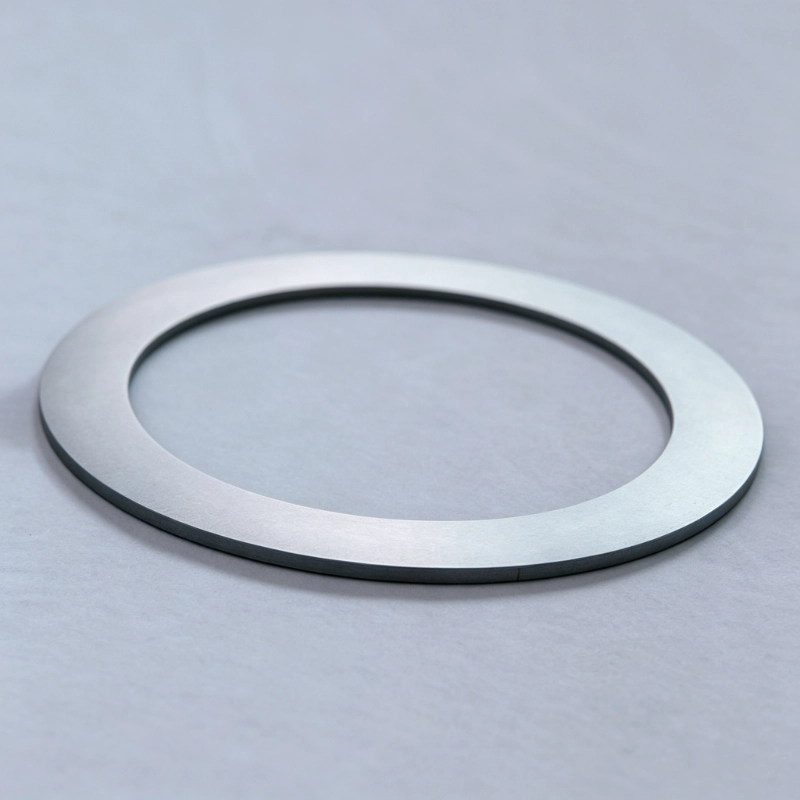
Silicon ring
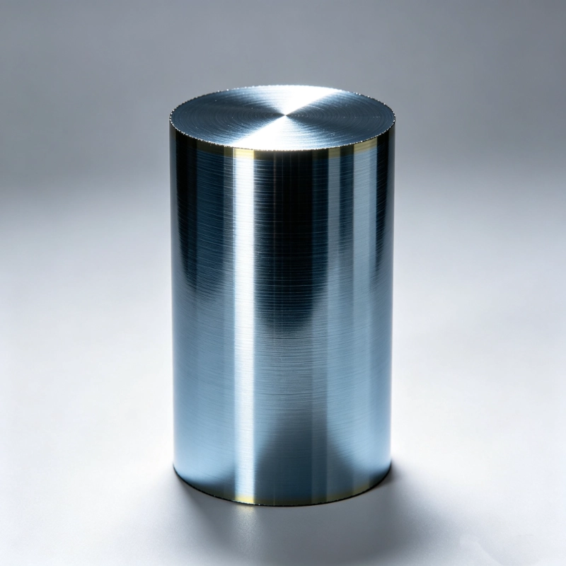
Silicon rods
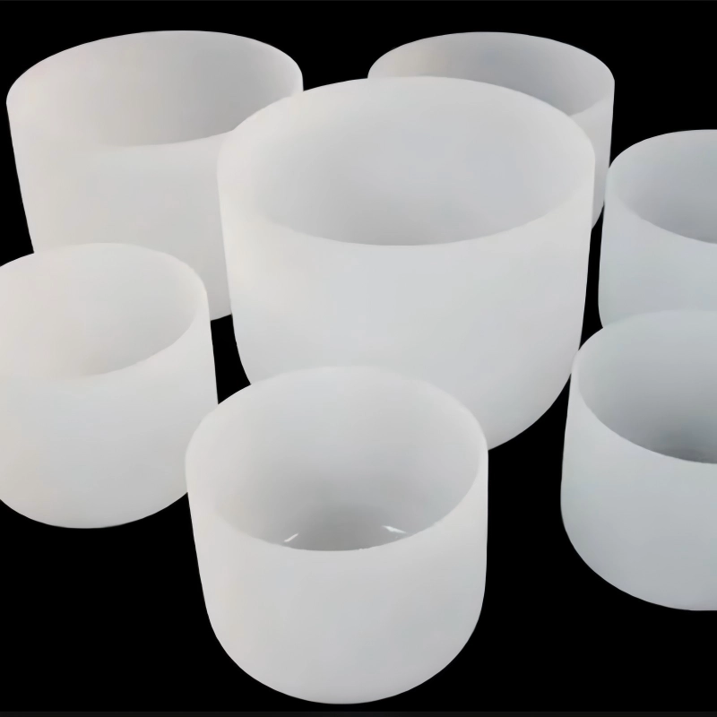
Quartz crucible
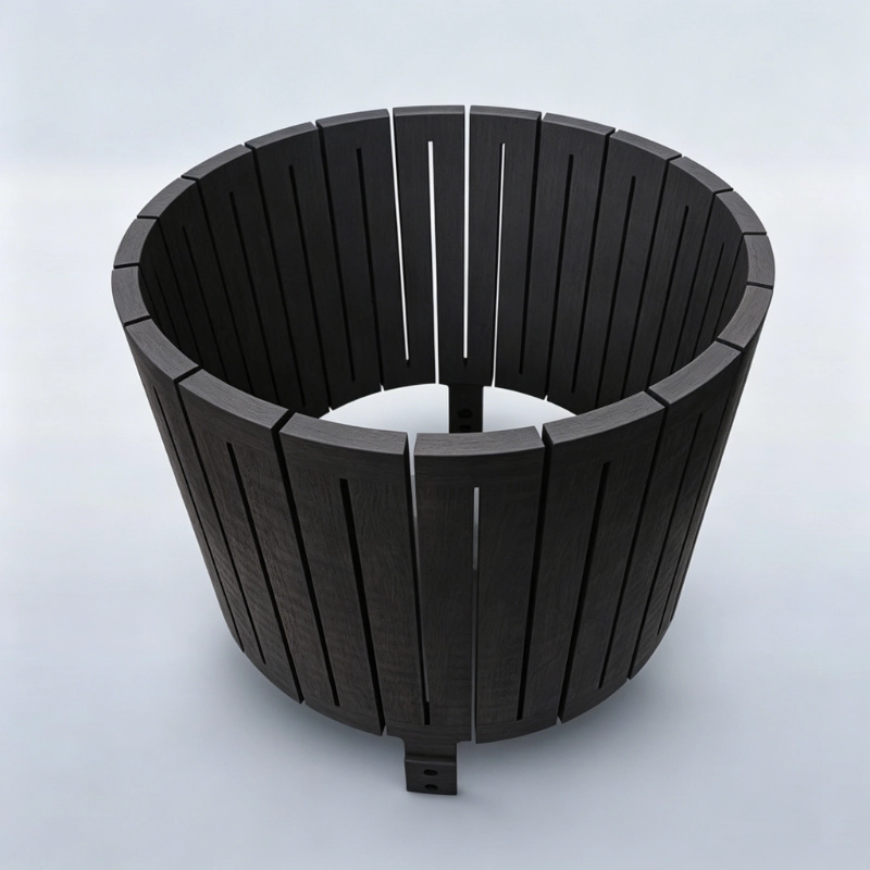
Graphite parts
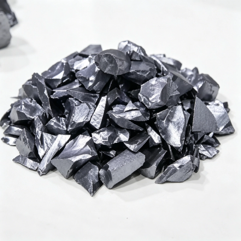
Electronic-grade polycrystalline silicon (bulk)
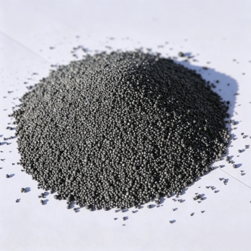
Electronic-grade polycrystalline silicon (particles)
News & Announcements
Recent Articles
 15th October 2026
Can a Small Batch Qualify Semiconductor Raw Materials?
 8th October 2026
Why Does Electronic Grade Polysilicon Price Vary?
 2nd October 2026
What Purity and Resistivity Data Should a High Purity Silicon Ingot Provide?
 10th September 2026
How Does a Quartz Crucible Affect Purity During Semiconductor Crystal Pulling?
 23rd September 2026
Why Does Silicon Wafer Price Vary for 8- and 12-Inch Sizes?
 17th September 2026
How Does a Silicon Focus Ring Improve Etch Uniformity?
Our Service
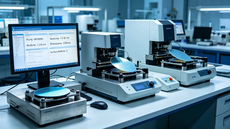
Quality testing services
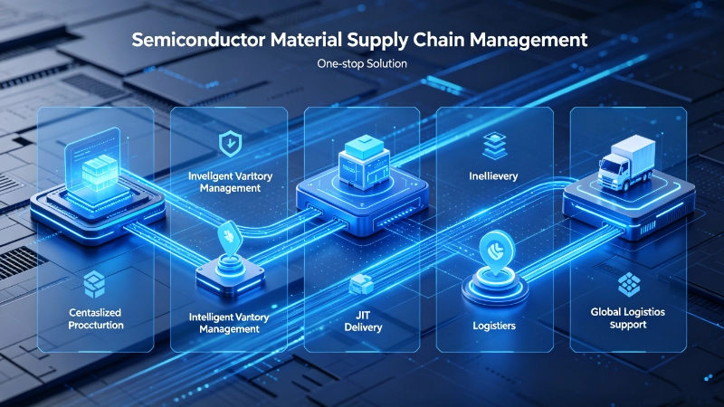
Supply chain management services

Partner with us for reliable semiconductor solutions.
Whether you need standard semiconductor materials or custom technical specifications, our expert engineering team is ready to help. Submit your requirements now and receive a detailed, professional quote within 24 hours.
Request A Quote