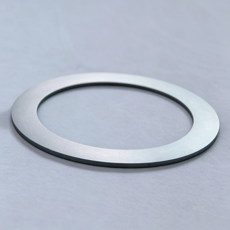
Silicon ring
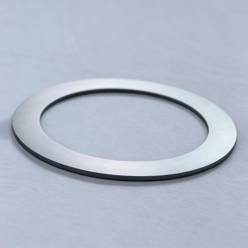
Our company's silicon ring products use high-purity single-crystal or polycrystalline silicon produced by advanced MCZ farad technology. They are manufactured through multiple precision machining processes including cutting, grinding, drilling, and polishing, achieving a purity of over 99.99999999%, dimensional accuracy within ±0.1 mm, and surface roughness below 0.1 micrometer. Product specifications cover various sizes of focusing rings, protective rings, and edge rings for 2-inch to 12-inch etching equipment, and custom designs are also available.
Product Details
a).Product Features and Advantages
Ultra-High Purity: Our silicon rings use high-purity monocrystalline or polycrystalline silicon as raw material, achieving a purity of over 99.9999999%. Key metal impurities such as iron, copper, aluminum, calcium, and sodium are controlled to the level of one part per billion. As a low atomic number material, silicon does not release harmful metal ions that contaminate the wafer under plasma bombardment, ensuring the cleanliness of the etching process and product yield.
Excellent Plasma Corrosion Resistance: Monocrystalline silicon has a dense crystal structure and excellent resistance to plasma bombardment. In fluorine-based and chlorine-based etching gas plasma environments, a dense passivation layer forms on the surface of the silicon ring, effectively slowing down further corrosion and extending the lifespan of the silicon ring. Compared to quartz and ceramic materials, silicon rings offer better process compatibility and a lower particle generation rate in silicon-based etching processes.
Precision Machining: Our company is equipped with advanced CNC precision machining equipment, enabling us to control the dimensional accuracy of silicon rings to within ±0.1 mm and the surface roughness to below 0.1 micrometer. For products with extremely high requirements for shape and size, such as focusing rings, we employ multi-axis linkage machining technology to ensure that key indicators such as concentricity of inner and outer diameters, parallelism of end faces, and hole diameter position accuracy meet the original equipment manufacturer’s specifications.
Excellent Thermal and Electrical Conductivity: Monocrystalline silicon possesses excellent thermal conductivity (approximately 150 watts per Kelvin per meter) and appropriate electrical conductivity (adjustable resistivity). In plasma processes, silicon rings effectively conduct the heat generated by the process, preventing localized overheating; simultaneously, appropriate conductivity helps stabilize the plasma potential, reducing arc discharge and particle generation.
Customizable Coating Options: For special process environments with higher requirements for corrosion resistance, we offer silicon carbide coated silicon rings and tantalum carbide coated silicon rings. Silicon carbide coating forms a dense protective layer on the surface of the silicon ring through chemical vapor deposition, further enhancing its resistance to plasma corrosion and wear, extending its service life by more than 50%. Coating thickness and process parameters can be customized to meet specific customer needs.
Strong batch consistency: Our company implements a comprehensive quality control system from raw material selection to finished product testing. Each batch of silicon rings undergoes rigorous dimensional and visual inspections. Key indicators such as inner and outer diameters, thickness, flatness, surface roughness, and aperture location are meticulously recorded and traceable. Customers can confidently purchase and use in bulk, avoiding process instability caused by fluctuations in silicon ring quality.
Reduced operating costs: Thanks to superior product quality and stable process performance, our silicon rings offer a longer service life and lower particle generation rate. By reducing the frequency of silicon ring replacement and lowering defect density in the etching process, we effectively help customers reduce overall operating costs and improve overall equipment efficiency.
b) Product Parameters
Product: Silicon Ring
We provide both monocrystalline and polycrystalline silicon ring variants. Monocrystalline silicon rings start with high-purity monocrystalline silicon produced via the Czochralski process, whereas polycrystalline versions use high-purity polysilicon feedstock.
All items adopt a ring geometry and can be custom-built per customer drawings into focusing rings, shielding rings, edge rings, top rings, bottom rings and other functional styles.
Outer diameter covers 50 mm to 400 mm, compatible with equipment from 2-inch up to 16-inch specifications. Inner diameter is configurable based on project demands and generally 5–20 mm wider than the target wafer size. Thickness falls between 1 mm and 15 mm, defined by equipment layout and actual process conditions.
For dimensional precision: OD tolerance is held within ±0.1 mm, ID tolerance within ±0.1 mm and thickness tolerance within ±0.05 mm. Concentricity between inner and outer diameters is limited to maximum 0.1 mm, and end-face flatness shall not exceed 0.1 mm.
In terms of surface finish, polished surfaces attain roughness below 0.1 μm, while ground surfaces reach under 1.6 μm. We support machining of through holes and blind holes with diameters from 0.2 mm to 5 mm. Hole position accuracy is controlled within ±0.05 mm, ensuring smooth, burr-free hole walls.
Material purity differs by grade. Monocrystalline silicon rings achieve purity above 99.9999999%, and polycrystalline silicon rings exceed 99.9999%. Resistivity is adjustable upon request, covering 0.005 Ω·cm to 5000 Ω·cm. Customers may choose N-type or P-type conductivity. Available crystal orientations include standard <100>, <110> and <111> as required.
Coating options include silicon carbide and tantalum carbide layers. Silicon carbide coatings range 1–50 μm thick with purity exceeding 99.999%. Tantalum carbide coatings measure 1–20 μm in thickness and feature purity above 99.99%.
A full test report accompanies every silicon ring, documenting critical metrics including dimension measurements, material grade, resistivity, conductivity type and visual inspection results.
Application Areas/Scenarios
Plasma Etching Equipment: Silicon rings are the most widely used in plasma etching equipment. The focusing ring is installed around the wafer to focus the plasma and improve etching uniformity, preventing abrupt changes in etching rate at the wafer edge. The protective ring is installed around the focusing ring to protect the lower electrode and cavity walls from plasma bombardment. The edge ring supports and protects the wafer edge. Silicon rings are indispensable key components in various etching processes, including oxide etching, nitride etching, polysilicon etching, and metal etching. Our products are compatible with mainstream etching equipment brands such as Lam Research, Tokyo Electron, and Applied Materials.
Physical Vapor Deposition Equipment: In physical vapor deposition (PVD) processes, silicon rings can be used to protect the inner walls of the deposition chamber, preventing sputtered material from depositing on the chamber components. During sputtering, silicon rings can collect excess sputtered particles, simplifying the chamber cleaning process and extending equipment maintenance cycles.
Chemical Vapor Deposition (CVD) Equipment: In CVD processes, silicon rings can be used as wafer support rings or edge protection rings to prevent the deposited film from cladding or peeling off at the wafer edges, reducing particulate contamination. The purity and thermal stability of silicon rings ensure reliable performance in high-temperature deposition environments.
Ion Implantation Equipment: In ion implantation processes, silicon rings can be used as ion beam confinement rings or focusing rings to help control and focus the ion beam, improving implantation uniformity. The low sputtering rate of silicon rings reduces the risk of metal contamination caused by ion bombardment.
Epitaxial Growth Equipment: In epitaxial growth processes, silicon rings can be used to support substrate wafers or as edge protection rings to prevent uneven growth of the epitaxial layer at the wafer edges. Silicon rings and silicon substrates have similar coefficients of thermal expansion and thermal conductivity, providing good thermal matching.
FAQ
Q: What are the differences between monocrystalline and polycrystalline silicon rings? How should buyers select the appropriate type?
A: Monocrystalline silicon rings are manufactured from single-crystal silicon feedstock. This material delivers fewer impurities, uniform crystal structure and less particle formation. It fits high-end semiconductor production that demands stringent cleanliness and stable process performance. Polycrystalline silicon rings adopt polysilicon as base material. Impurity levels are moderately higher compared with monocrystalline alternatives, yet they carry a cost advantage. This variant works well for cost-conscious scenarios or applications with frequent component replacement. As a general guideline, monocrystalline silicon rings are preferred for advanced and critical manufacturing steps. Polycrystalline silicon rings offer a practical option for mature, non-critical processes or high-consumption positions to lower overall operational expenses.
Q: What is the lifespan of a silicon ring? How is the replacement cycle determined?
A: The lifespan of a silicon ring is affected by various factors, including the type of etching gas, plasma power density, process temperature, silicon ring material, and design requirements. In typical etching processes, the lifespan of a focusing ring is typically between 5,000 and 20,000 wafers processed, while the lifespan of a guard ring is typically longer because it is farther from the plasma center. Users are advised to determine the replacement timing based on a comprehensive assessment of the equipment manufacturer’s recommended replacement cycle, silicon ring visual inspection (e.g., corrosion depth, surface condition), and process monitoring data (e.g., changes in etching rate, uniformity, and defect monitoring results).
Q: Can silicon rings be recycled after use?
A: Used silicon rings have undergone plasma corrosion, and some areas may have formed corrosion pits or discoloration, making them generally unsuitable for direct recycling for use in the same level of process. However, recycled silicon rings can be remelted as raw materials for the production of polycrystalline silicon ingots or low-purity silicon components. Some customers return used silicon rings to their suppliers for material recycling. Our company can provide recycling solutions for used silicon rings for customers who require them; please consult our sales team for details.
Q: What are the advantages of silicon carbide coated silicon rings compared to ordinary silicon rings?
A: Silicon carbide coated silicon rings form a dense silicon carbide protective layer on the surface of the silicon ring through a chemical vapor deposition process. Silicon carbide has higher hardness, superior resistance to plasma corrosion, and better oxidation resistance. Compared to ordinary silicon rings, silicon carbide-coated silicon rings exhibit a 50% to 80% reduction in corrosion rate in fluorine-based plasma environments, and their service life can be more than doubled. Furthermore, the low particle generation characteristic of the silicon carbide coating helps reduce wafer defect density. However, silicon carbide-coated silicon rings are more expensive and are suitable for applications with harsh process conditions, frequent replacements, or strict particle control requirements. Tantalum carbide coatings, on the other hand, offer higher corrosion resistance and are suitable for more corrosive process environments such as chlorine-based processes.
Q: How does the dimensional accuracy of the silicon ring affect the process?
A: The dimensional accuracy of the silicon ring directly affects the edge uniformity and defect level of the etching process. If the inner diameter of the silicon ring is too large, the plasma distribution in the wafer edge region will change, leading to abnormal edge etching rates. If the inner diameter of the silicon ring is too small, it may cause the wafer to not be properly placed or result in contact damage. If the silicon ring thickness is uneven or the flatness is poor, it may lead to unstable wafer support or localized stress. Insufficient aperture positioning accuracy will affect the gas flow field distribution of the equipment. Therefore, our company strictly controls the dimensional accuracy of the silicon rings to ensure complete matching with the original equipment manufacturer’s specifications, providing customers with reliable process assurance.
Q: Do you provide sample testing for silicon rings?
A: Yes, we support customers requesting silicon ring samples for testing. Sample specifications can be provided in standard or customized sizes according to customer needs. The sample quantity is usually two to five pieces. Please contact our sales team for specific application procedures and conditions. We provide technical support to assist customers in completing on-machine testing and process verification.

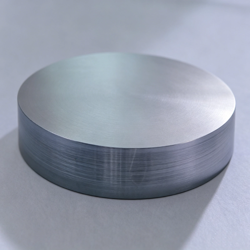
Silicon Wafers
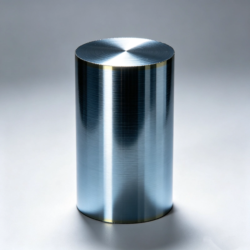
Silicon rods
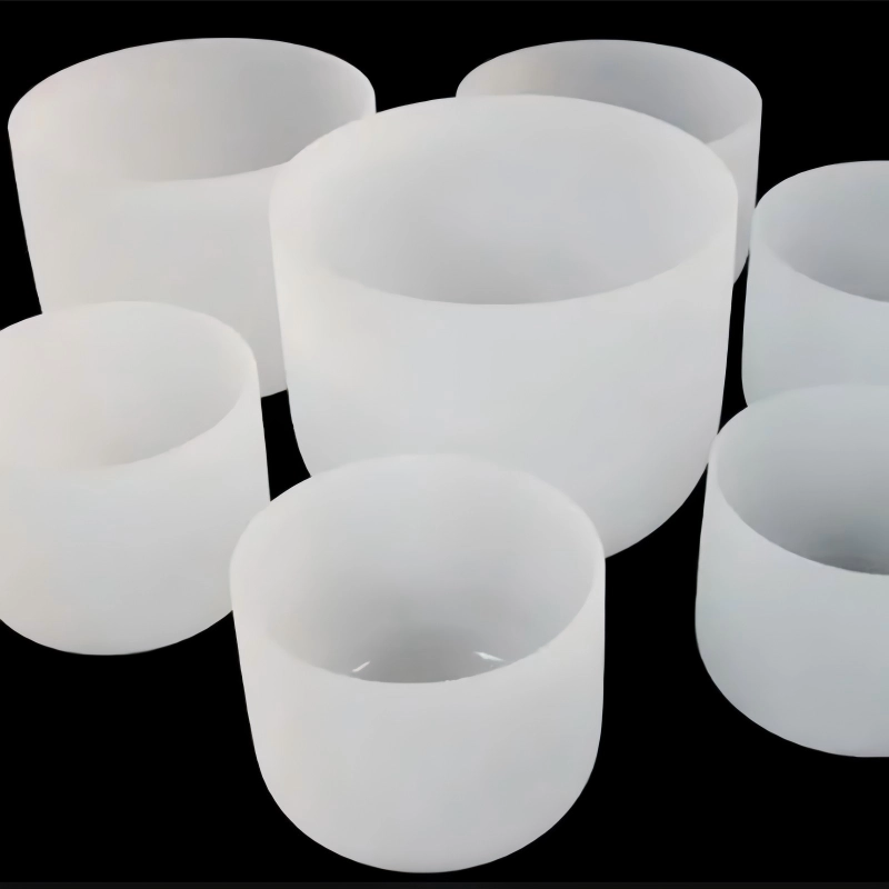
Quartz crucible
Graphite parts
Electronic-grade polycrystalline silicon (bulk)
Electronic-grade polycrystalline silicon (particles)
News & Announcements
Recent Articles
 15th October 2026
Can a Small Batch Qualify Semiconductor Raw Materials?
 8th October 2026
Why Does Electronic Grade Polysilicon Price Vary?
 2nd October 2026
What Purity and Resistivity Data Should a High Purity Silicon Ingot Provide?
 10th September 2026
How Does a Quartz Crucible Affect Purity During Semiconductor Crystal Pulling?
 23rd September 2026
Why Does Silicon Wafer Price Vary for 8- and 12-Inch Sizes?
 17th September 2026
How Does a Silicon Focus Ring Improve Etch Uniformity?
Our Service
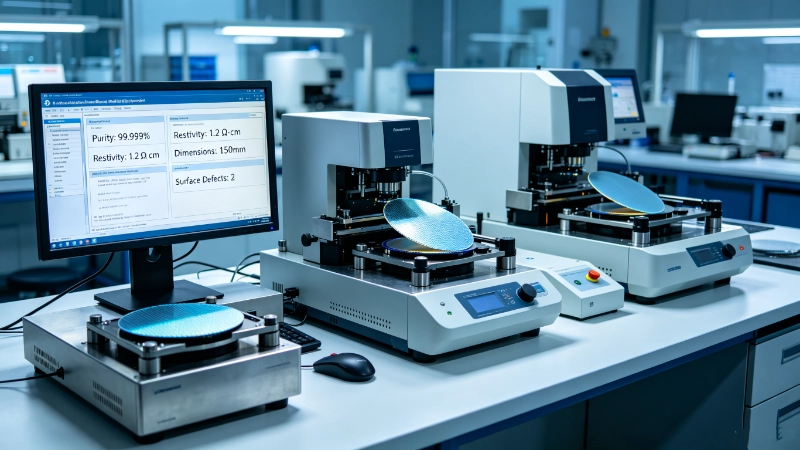
Quality testing services
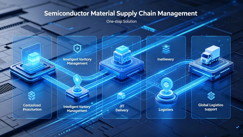
Supply chain management services

Partner with us for reliable semiconductor solutions.
Whether you need standard semiconductor materials or custom technical specifications, our expert engineering team is ready to help. Submit your requirements now and receive a detailed, professional quote within 24 hours.
Request A Quote