What Purity and Resistivity Data Should a High Purity Silicon Ingot Provide?
-
 author
- 2nd October 2026
Buying a high purity silicon ingot for semiconductor processing is not a matter of accepting a single purity percentage. Before slicing and polishing, a buyer needs a traceable data set connecting the ingot to the intended wafer, device process, and inspection plan. Purity, resistivity, conductivity type, crystal orientation, dimensions, and lot evidence work together. If one field is missing, later wafer results become harder to explain or compare.
Begin With the Intended Downstream Process
The right specification depends on what the material will become. A wafer for a device line may need a particular conductivity type and resistivity window, while an evaluation lot may be judged first on diameter, orientation, surface condition, and documentation. A buyer should state the target process, wafer diameter, and expected order stage before asking for a quote.
That context prevents a common mistake: treating “high purity” as a universal grade. Purity does not by itself define electrical behavior or crystal suitability. A supplier should explain which values are controlled at the ingot stage and which are verified after slicing.

What Purity Data Should Be Reported?
Purity data should identify the measurement basis, relevant impurity families, and the lot or ingot covered. A certificate that states only “high purity” is difficult to audit. Request reported values or ranges, the test method or laboratory reference, the sample location when relevant, and the lot identifier.
Trace elements matter because a small concentration can affect crystal growth or downstream device behavior. The practical goal is not to collect an impressive table that no one uses. It is to define the impurity limits that matter for the intended process and to make sure the certificate maps to the material being shipped. The semiconductor raw materials range provides the product context for buyers comparing polysilicon and related feedstock before an ingot is qualified.
Purity evidence should also be consistent across documents. The commercial quotation, certificate of analysis, packing label, and internal receiving record should use the same product description and lot number. This is where a supplier’s traceability process becomes as important as the headline purity claim.
Resistivity and Conductivity Type Are Separate Decisions
Resistivity describes how strongly the material opposes electrical current, while conductivity type identifies whether the silicon is n-type or p-type. The two fields should appear together in a technical discussion, but they are not interchangeable. A buyer who specifies only “high resistivity” has not defined the required electrical behavior.
Ask for the nominal value, tolerance or range, measurement temperature, test orientation, and the method used to calculate or measure the result. If a value is supplied from a sample rather than the full ingot, that limitation should be explicit. The same rule applies to conductivity type: the certificate should state the type and show how it was verified.
For custom material, a supplier should explain how the requested range will be checked before shipment and what happens if a lot falls outside the agreed window. That answer is more useful than an isolated number because it connects the specification to acceptance and corrective action.

Geometry and Crystal Information Complete the Picture
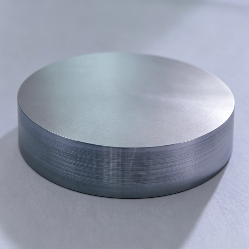
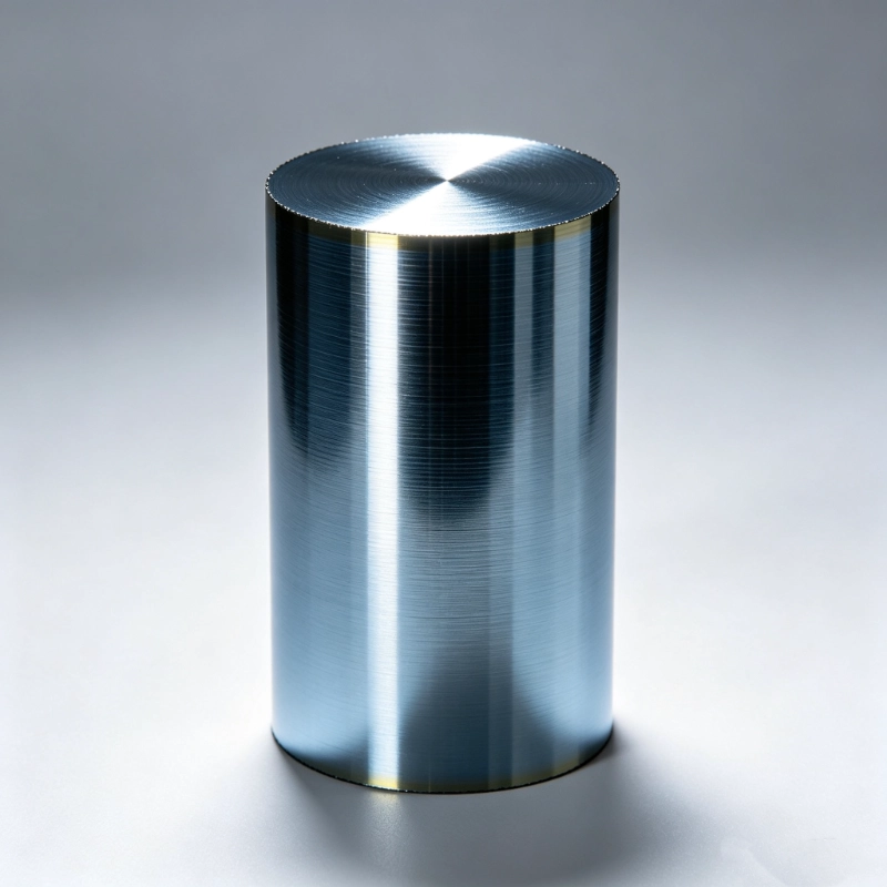
An ingot specification should describe diameter, usable length, crystal orientation, and any relevant end or surface condition. These fields affect how efficiently the material can be sliced and whether the resulting wafers match the buyer’s fixtures and process assumptions. If a customer needs a particular diameter or orientation, the requirement should appear in the purchase specification rather than remain in an email thread.
The silicon rod product information is a useful reference point for discussing diameter and crystal form. Buyers should confirm which dimensions are nominal, which are guaranteed, and where measurement points are located. A clear drawing or inspection sketch can prevent disputes when a cylindrical surface, usable length, or end section is interpreted differently by two teams.
How Should the Certificate Be Linked to the Lot?
Every certificate should identify the material with a lot number that appears on packaging and shipping documents. The record should be easy to follow from incoming inspection to wafer conversion. At minimum, retain the quotation, approved specification, certificate of analysis, packing list, inspection result, and any deviation approval together.
This evidence chain is especially important for small evaluation orders. A sample that performs well is valuable only when the buyer can request the same grade again and understand what changed, if anything. A supplier that can support flexible quantities should still preserve the same discipline for a small lot as for a volume shipment.
Use Independent Testing for Critical Attributes
Supplier certificates are essential, but critical applications may require confirmation through an agreed inspection plan. Define which tests are released by the supplier, which are checked by the buyer, and which can be handled by an independent laboratory. The quality testing service can be part of that conversation when the project needs additional evidence for purity, electrical properties, dimensions, or surface condition.
Testing should be proportionate to the decision. Repeating every measurement on every shipment may be unnecessary, while skipping a critical attribute can create a costly failure. Combine certificate review, incoming sampling, and periodic independent verification around the highest risks.
Align Supply and Change Control
Technical data loses value when the supply process changes without notice. Ask how a supplier handles raw-material, site, equipment, and measurement-method changes. The buyer should know which changes require requalification and which can be routine notifications.
THE EQUATOR supports semiconductor material sourcing and related supply-chain coordination, so buyers can discuss nominated factories, evaluation quantities, and document control through its supply chain management service. The purpose is not to add paperwork for its own sake. It is to keep the approved material definition stable while the order moves from evaluation to production.
img. Silicon material quality testing service.webp
A Practical Data Package for Approval
A useful high purity silicon ingot package answers five questions: what material is this, what electrical behavior should it have, what geometry will arrive, how was it tested, and how can the lot be traced? When aligned, those answers let a buyer compare suppliers on evidence rather than adjectives.
Before placing an order, send the intended wafer diameter, conductivity type, resistivity window, orientation, purity limits, inspection points, packaging needs, and change-notification rules. Then ask the supplier to return the same fields in the quotation and certificate. That simple alignment makes later wafer results easier to interpret and gives both sides a defensible acceptance basis.
FAQs
Q: Is a purity percentage enough to qualify a high purity silicon ingot?
A: No. The buyer also needs impurity details, electrical information, geometry, crystal orientation, lot identification, and the measurement basis. A single percentage cannot show whether the ingot fits the intended wafer process.
Q: What is the difference between resistivity and conductivity type?
A: Conductivity type identifies n-type or p-type silicon. Resistivity describes the material’s opposition to current and should be specified with a value and tolerance. Both fields should be reviewed together because one does not replace the other.
Q: When should a buyer request independent testing?
A: Use independent testing when the attribute is critical to device performance, when a new supplier or factory is being qualified, or when the certificate does not provide enough method and lot detail. The testing plan should be agreed before shipment.

Silicon Wafers
Silicon ring
Silicon rods
Quartz crucible
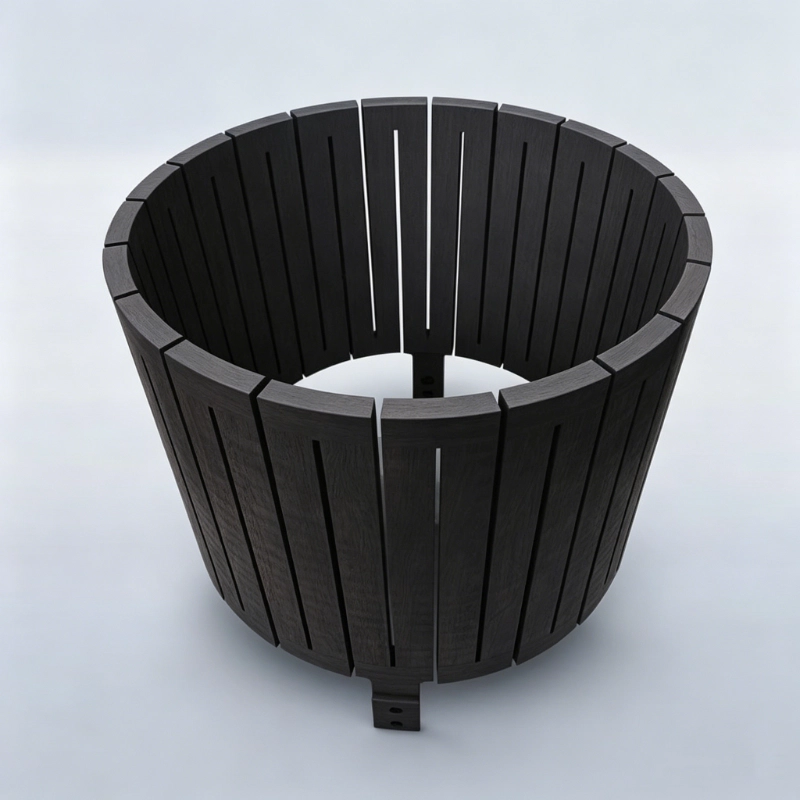
Graphite parts
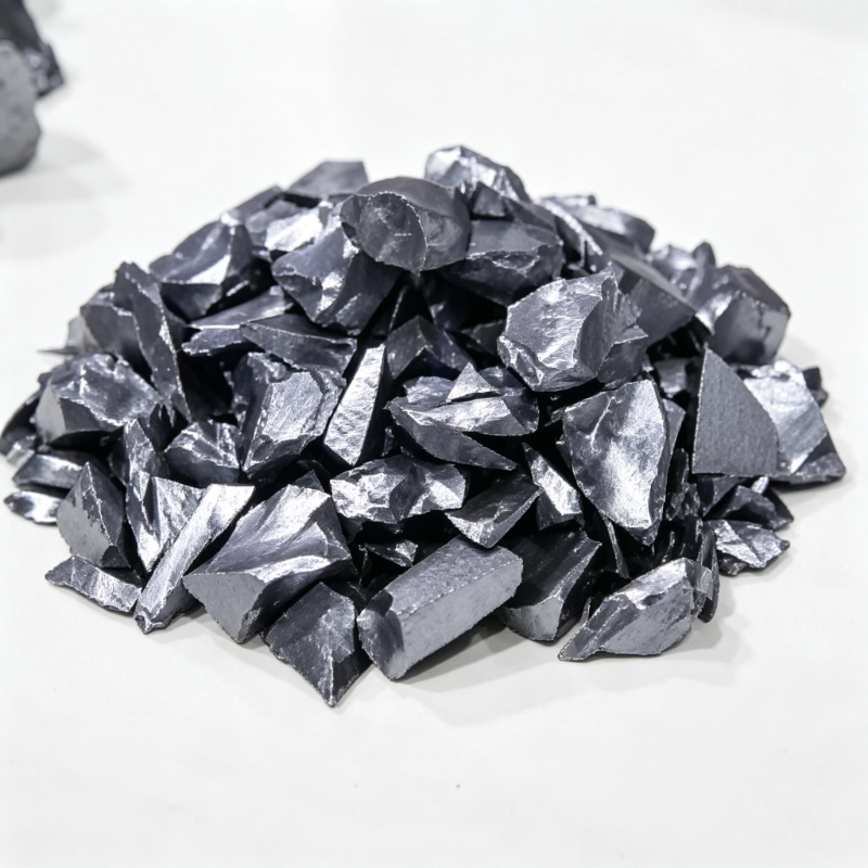
Electronic-grade polycrystalline silicon (bulk)

Partner with us for reliable semiconductor solutions.
Whether you need standard semiconductor materials or custom technical specifications, our expert engineering team is ready to help. Submit your requirements now and receive a detailed, professional quote within 24 hours.
Request A Quote